Von Neumann Bottleneck
There has been an improvement in the number of transistors on a chip. More transistors mean that we have increased our ability to store more memory in less physical space. Memory storage is more efficient than ever.
Today, AI and machine learning are being studied. This requires us to store and process a large density of data, which is possible given the environment: processors and storage solutions. Also, Von Neumann Architecture requires us to store data in a separate block, and the processor needs an individual block. These different blocks are connected by buses. Given this architecture, to process these large-density data, the transfer rates must also be at par with the processing speed, maybe even faster. However, over the years, the increase in transfer speedhas only made a few gains.
When the processor has to stay idle to fetch the data from the memory block, this condition is called the Von-Neumann Bottleneck.
Some attempts to surpass this limitation have been made like:
Caching: Chaches are temporary storage units between the main memory block and the processor. It can store a subset of data so that future requests for that data can be served faster. For example, they store results of earlier computations or a copy of data stored elsewhere.
Hardware Acceleration: Hardware like GPUs, FPGAs, and ASICs are brought into the picture for faster response from the hardware side.
But these come with some limitations:
Limitations of Caching:
Size: Larger caches increase hit rates but consume more silicon area and power.
In multicore systems, maintaining consistency across caches is difficult.
Memory Latency and Bandwidth Issues: If the working set exceeds capacity, frequent primary memory access still causes stalls.
Hardware Accelerators’ Limitations:
Domain-Specificity: FPGAs, TPUs, and GPUs lack generality. They are often made for specific tasks, which, economically speaking, makes them challenging to produce.
At the end of the day, communications are still being made over buses, so the transfer limitation persists.
Software and Compatibility Issues: These devices run on specific firmware and can cause compatibility issues.
Power and Heat Management: These hardware accelerators generate much heat and consume much power, which obviously isn’t preferable.
Now, we dive into analog methods of overcoming this phenomenon. Of course, some digital methods have been proposed but let’s stick to the title of the blog for now and maybe (definitely) I’ll discuss digital methods in a future blog.
Analog Implementation of MACS
MAC, or Multiply-Accumulate Operation, is a common step which computes the product of two numbers and adds that product to an accumulator. MAC operations account for over 90% of Neural Network and AI computations. Yeah, so they are “kind of” important.
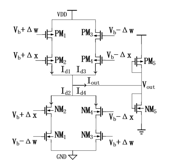
In the following circuit, we have 10 MOSFETs in total (5 PMOS, 5 CMOS), let us label them: PM1, PM2, PM3, PM4, PM5, NM1, NM2, NM3, NM4, NM5.
These MOSFETs are linearly biased (if you somewhat unfamiliar with working of MOSFET, go watch Engineering Mindset’s video on MOSFET on YouTube, I found it very good for a quick get around). We are applying differential inputs $+\Delta x, -\Delta x, +\Delta w , -\Delta w$.
The given transistors are now arranged in the following circuit (Image Courtesy: Reference [1]):
Now, let’s get into some transistor math.
Since, all the transistors are operating in linear region, drain current Id2 is given by:
$I_{d2} =K_{n}*[V_{b}-\Delta w - V_{thn} - \frac{V_{b} + \Delta x}{2}]*(V_{b}+\Delta x)$
For knowing what each term means, refer to [1].
Now, we are taking the transconductance factors and threshold voltages of the N and P MOSFETS to be equal, we get the following expression for the output current:
$I_{out} = 4*K*\Delta w * \Delta x$
If you observer the above expression, we have multiplied two numbers! Now, all we have left to do is accumulate.
The load MOSFETS: PM5 and NM5 can seen as an equivalent load resistor, which will convert the output current to an output voltage:
$\Delta y = V_{out}-V_{outbias}$
This can be easily visualized in the figure below:
![Image Courtesy : [1]](/images/2.png)
Now, closely look at the (b) part of the above image, what we are doing is we are adding output currents of multiple sources (or I should say multipliers), such that the output voltage can be given by:
$V = \frac{1}{N}*\sum_{i=1}^{N} I_{i}*R_{load}$
With this, we have successfully created our analog MAC unit. Let us end this part-1 here. Next part, we will delve into experimental results, architecture, and maybe hybrid models proposed.
peace. da1729
References
[1] J. Zhu, B. Chen, Z. Yang, L. Meng and T. T. Ye, “Analog Circuit Implementation of Neural Networks for In-Sensor Computing,” 2021 IEEE Computer Society Annual Symposium on VLSI (ISVLSI), Tampa, FL, USA, 2021, pp. 150-156, doi: 10.1109/ISVLSI51109.2021.00037. keywords: {Convolution;Neural networks;Linearity;Analog circuits;Very large scale integration;CMOS process;Silicon;Analog Computing;In-Sensor Computing;Edge Computing},
[2] Robert Sheldon, “von Neumann bottleneck”, TechTarget, https://www.techtarget.com/whatis/definition/von-Neumann-bottleneck#:~:text=The%20von%20Neumann%20bottleneck%20is,processing%20while%20they%20were%20running.